
What
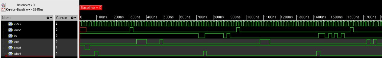
This four-bit multiplier was designed for a VLSI class project. The requirements were to make a four-bit serial in/serial out multiplier that accepts data when start is asserted and asserts the done flag when the result is being outputted. This is all possible thanks to an FSM that transitions between a few states (IDLE, S2P, MULT, P2S, DONE). The project entailed designing the multiplier in Verilog, testbenching the design in SimVision, synthesizing the design in Genus and doing place and route in Innovus.

How
The process started by designing the FSM and drawing the state transition diagram. From there, the FSM could be implemented in Verilog along with the four-bit multiplier which was implemented structurally to better understand the design process behind the software. After the RTL was complete, I needed to verify it was behaving properly so I built a self-checking testbench to confirm it. After some debug, the next step was synthesizing the design and starting the place and route in Cadence Innovus. The Inovus process focused on minimizing design area, providing enough taps and running clock tree synthesis to minimize uneven skew. With the placed design I also harvested the maximum delay paths and power consumption. From this I calculated the maximum clock rate my design can meet timing closure at: 173 MHz.
Reflection
After completing this project I gained a better understanding of how the design process goes from RTL to GDS-II. This project helped me strengthen my RTL + testbench skills as well as improve my pnr skills. After getting more experience with pnr I can see that my placement was a bit inefficient as I had some empty space leftover where I had to place filler cells. Otherwise, a fun addition for this project in the future would be making it bus protocol compliant, such as AXI-4 compliant. AXI-4 is one of the more popular protocols in the FPGA space and has many versions to best fit your project's needs.